RANT + INTRO
I had the thought of writing the blog because I see so many people learning and teaching only the rules of electronics design and printed circuit board design. But very few talk about the WHY. I wanted to talk about the WHY things happen. WHY some boards have crappy emission (EMI EMC). Why does doing the EMI EMC matter. So once we understand the WHY, then sorting out the HOW seems much more logical and solutions will come much easier.
I want to start with one great quote I heard from Rick which we heard from Lee Richie.
Circuit application notes produced by IC manufacturer should be assumed wrong until proven right !
– Lee Richie
STORY
In 1992, a tragic incident highlighted the importance of EMI/EMC considerations. Medical technicians were transporting a heart attack victim to the hospital. They used a monitor/defibrillator, but each time they activated their radio transmitter for assistance, the heart machine shut down, ultimately leading to the patient’s demise. The cause? The ambulance’s roof had been replaced with fiberglass and equipped with a long-range radio antenna, significantly reducing the shielding. The strong radio signals interfered with the monitor unit, rendering it useless.
This incident serves as a stark reminder of the potential dangers posed by electromagnetic radiation. Today, stringent EMI/EMC compliance standards are in place to ensure the safety of electronic equipment.
THE CRUX OF THE MATTER:
As design engineers, we spend a lot of time understanding circuit theory. However, 95% of us do not fully grasp PCB layout. Mostly because it’s handled by different layout engineers, and the only effort we spend is to check the layout against the rules set by the IC manufacturer. This is the cardinal sin. Our boards start to fail due to negligence in PCB design. We obsess over 90-degree corners, which are of minor concern, but in most designs, the failure is not because of that.
What are the things that you should really care about? The rise time of the signals on the board. Please let go of the concept that clock frequency causes EMC problems. Secondly, everything you design should be with controlled impedance, whether you buy it as controlled impedance or not.
When the propagation time exceeds 1/4 of the rise time, your circuit will start to experience reflections, ringing, and that’s when you’ll see an increase in crosstalk, EMI, and all the issues that plague us when the line is long enough. How long is long enough?
Let me introduce you to transmission-line basics. Lumped elements, for example:
- 5MHz Clock with a rise time of 100ns = Lumped element length is approximately 3 meters (120,000 mils).
- 20MHz Clock with a 10ns+ rise time = Lumped element length is approximately 45cm (17,716 mils) to 100cm (39,370 mils).
- Today’s circuits typically have 100 MHz to 1 GHz clocks with rise times ranging from 2ns to 100ps = Lumped element lengths from 4mm (157 mils) to 75mm (2,952 mils).
In the current world of electronics circuit design, anything above 4mm to 3 inches can be a possible point of issue for EMI in your next board design. Sadly, this critical information can’t be seen in most datasheets. Our lives have been hampered by manufacturers not providing us with the critical data we need to identify potential problems. So, what do you do? Luckily, the answer lies in the spice models of the ICs. You can obtain rise time data by digging up these models.
To discuss other issues we encounter in PCB design, we always match the lengths of high-speed signals. But in reality, you should match the propagation time of the transmission lines (traces). This is because outer layers propagate at a different speed than inner layers, and heavily loaded traces propagate slower than lightly loaded ones.
Understanding Distributed Line Length for Digital Signals:
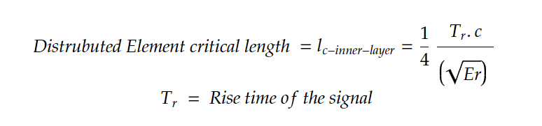
The equation for calculating critical lengths for digital signals (Distributed line length):
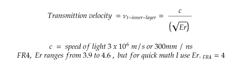
This equation gives typical propagation velocities of approximately 6 inches per nanosecond in the inner layer of the PCB. To this equation, add the rise time and the constant 1/4 because, at 1/4th the rise time, we start to see reflections and other undesirable effects.
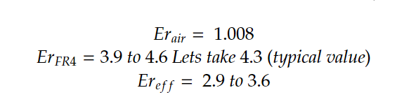
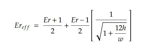
For the outer layer, the equation remains almost the same, but there is a slight variation in how the Er (Dielectric Constant or Relative Permittivity) is calculated, as we have to consider both the air above the PCB and the dielectric the PCB is constructed with.
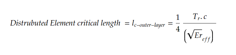
This means that energy transmits 15% to 20% faster on outer layers. So, to conclude, STOP MATCHING LENGTHS and start matching propagation times. When matching the outer layer traces, they should be 15% to 20% longer, depending on the materials used.
For those curious about how to calculate the effective Relative Permittivity, it’s recommended to use field solver tools. However, for most of us, these tools might be out of reach.
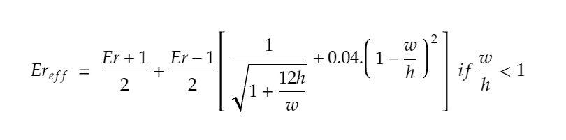
For all practical conditions where we want to achieve a 50Ω or 100Ω impedance match, the w/h ratio will always be greater than 1. So most of the time you can stick to the simpler equation below
The equation might look intriguing but it’s fairly simple. Let me give a practical table for reference
| Device Type | Rise time | Max length – Inner layer | Max length – Outer layer |
| Std TTL | 5.0 ns | 7.2 Inches | 8.3 Inches |
| Schottky TTL | 3.0 ns | 4.36 Inches | 4.17 Inches |
| 10k ECL | 2.5 ns | 3.63 Inches | 4.17 Inches |
| ASTTL | 1.9 ns | 2.76 Inches | 3.17 Inches |
| FTTL | 1.2 ns | 1.75 Inches | 2.00 Inches |
| BICMOS | 0.7 ns | 1.02 Inches | 1.17 Inches |
| 10KH ECL | 0.7 ns | 1.02 Inches | 1.17 Inches |
| 100K ECL | 0.5 ns | 0.73 Inches | 0.83 Inches |
| GaAs | 0.3 ns | 0.44 Inches | 0.50 Inches |
Understanding Distributed Line Length for Analog Signals:
For analog signals, the frequency of the clock doesn’t matter as it does for digital signals. Why? Because an analog signal is always a sine wave, while a digital signal is never a sine wave. The distributed length of analog signals is a function of the wavelength in a specific conducting material, which largely depends on the Relative Permittivity of the material.
The equation for calculating critical lengths for analog signals (Distributed line length):
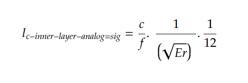
c = speed of light , f = frequency of the signal Er = dielectric constant or Relative Permittivity
For a Stripline trace (inner layer trace), if a 1GHz signal travels in an FR4 material, as long as the trace length is above 480 mils, EMI is not a significant concern.
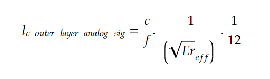
Similarly For the Micro strip = (read outer layer trace), replace the Er with Ereff, So for a 1GHz signal traveling on the outer layer of a FR4 material, till the trace length is above 530mils we are all good with EMI.
TO CONCLUDE:
What do all these lengths mean? If the rise time of the signal you are working with doesn’t exceed the critical lumped length, it cannot act as an antenna and cannot cause issues by emitting signals from the copper lines. So, if it’s less than this length, you don’t have to worry about impedance matching, terminations, stubs, and all the complex rules that everyone says will cause problems. But when it exceeds these limits, it can be a buzzkill both in the EMC labs and in real-life, just like in the story in the intro. So, design your circuits with the right layout.
To be Continued…
Be First to Comment