On my last blog (Part-1) I quoted, “an analog signal is always a sine wave and the digital signal is never a sine wave.” Let me tell you something straight up, that was a lie. So if you don’t have an idea of what I am talking about, please do yourself a favor and check PART-1.
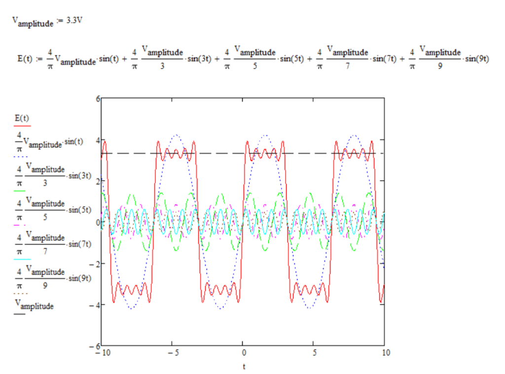
That brings us to the question: WHAT is a digital square wave? Fact 1: All practical square waves are Trapezoidal shaped waves. Fact 2: They are the algebraic sum of many sine waves, or better, the sum of harmonics of a sine wave. If you would like to do a deep dive on how the math works, please follow this link from “www.allaboutcircuits.com” -> Square Wave Signals.
Thanks to: Werner_E 24-Ruby IV for the video: If you do the math enough times. 😀 (Replay the video’s first few seconds to see the impact fully, The changes after the few seconds are not that evident)
I hope you get the idea. So as the rise time and fall time of the signal get faster, the amplitude of the harmonics also increases. Suddenly you are dealing with antennas on every line of your PCB board.
What do all these mean?
-
- The highest frequency that we have to worry about is not the clock.
-
- All we have to worry about is the frequency of the harmonic which creates the fast rising edge of the square wave.
-
- This frequency is called the Maximum Pulse Frequency.
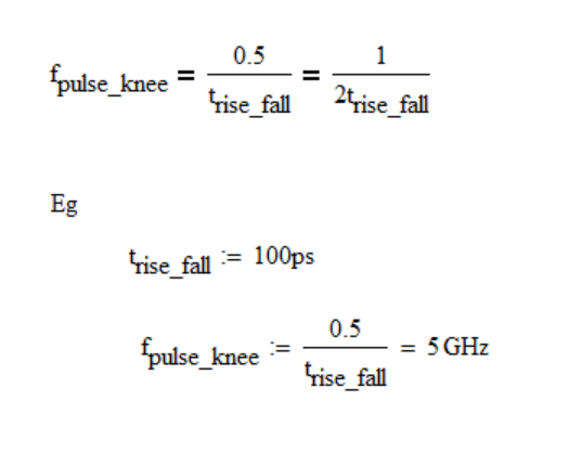
NOTE: As per the textbook definition – Maximum Pulse Frequency’s Knee power is at about 0.35, but industry experts like Rick Hartly, Ken Wyatt, etc., have been preaching it’s better to take it as 0.5 for all EMI-related calculations. It means that even if we have a slow clock signal, maybe in 100kHz frequency, if the rise time of the clock is 100ps, then we have to deal with possible EMI radiations due to a frequency ranging from 100kHz to 5GHz.
HOW is the ENERGY of the signal TRANSMITTED?
To understand this, we need some transmission-line basics. (All those boring college classes coming back to haunt us.) Let me state a few facts quickly.
-
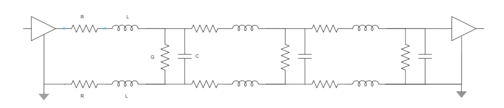
- A transmission line is any pair of conductors or wires used to move energy from point A to Point B.
-
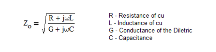
- All transmission lines have Impedance (Zo), the resistance that it provides against moving energy from Point A to point B.
-
- By controlling the size of the conductor or the dielectric, it’s possible to control the Impedance (Zo).
So we understand a bit of the road through which the energy is transmitted, obviously, the road being the transmission line. So what exactly are we transmitting? Where is the energy in the circuit board? Is it in the Voltage or Is it the Current? The answer to this is where college messed us up. Please throw away that water reservoir analogy and take this for a fact. Energy is neither in the voltage nor in the current. It’s in the field.
Let me explain, the first thing we have to understand is both electrical energy and light energy are identical. Both are electromagnetic waves. The only difference is the frequency. So because it’s an electromagnetic wave, it has two fields, the Electric field (E) and the magnetic field (B).
Coming back to our main question, where is the energy in the circuit board. Is it in the copper traces, where the current flows? or the larger copper pours we call planes? The answer to this question blew my mind. It changes the way I see circuit board design.
The energy does NOT travel either in the copper traces or in the copper planes, but in the dielectric between them. Let me reiterate this. This is the most important point I want to drive. The energy of the signals is transmitted through the plastic and fiberglass (non-conducting materials sandwiched between the copper planes).
So the transmission line constitutes the traces, planes, and dielectrics. The traces steer the energy from point A to point B. The copper elements act as wave guides. Hey, aren’t the wave guides designed for those RF engineers? Knowingly or unknowingly, we have been designing wave guides all this time along.
Understanding Characteristic Impedance of the transmission line
[ Derivation of the Characteristic impedance check wiki link -> Characteristic impedance derivation ]
For all practical applications, below 1GHz the R and G can be neglected. But if you are dealing with frequencies above 1GHz, then considerations with the conductance of the material come into play, generally noted by the PCB manufacturer as loss tangent, which is the inverse of the conductance of the material. i.e., for really high frequencies, the dielectric material absorbs some of the energy, so care has to be taken when choosing a dielectric material with a lower loss tangent. So for all digital signals under 1GHz, we could simplify the equation.
Component 1 – Inductance: As per definition – The Inductance is the impedance (read – resistance towards something) to the change in current flow caused by the mass of the magnetic field. Throwing some light to college days, remember Ampere’s Law, which states that when a current is flowing through a conductor wire, a magnetic field is generated near the space around it. This magnetic field will try to keep the current flowing and try to limit any change to the flow of current. This property of a wire or a coil that tries to sustain the flow of current is called Inductance.
What does it mean for our transmission line? When a current is flowing through the conductor, it will generate a magnetic field around the conductor. The size of the magnetic field defines the inductance of the transmission line. When we try using energy through the field, this resistance from the inductor element of the transmission line will delay the change in energy, causing a voltage drop across the transmission line. So if we want to transfer energy over a trace fast (transmission line), then we want to keep the inductance of the element as low as possible.
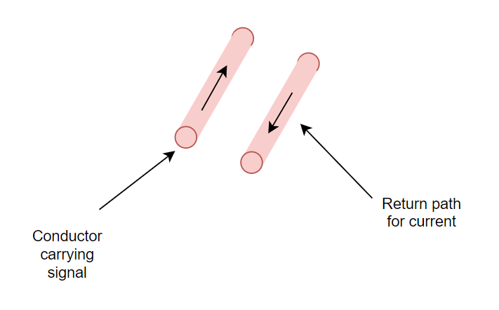
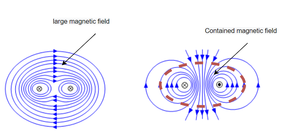
Based on some prior information from school physics -> [link Forces between currents], when we have current traveling in the opposite directions, the fields concentrate between the conductors, reducing the inductance of the line. i.e., why we want to have reference paths or return paths (generally called ground paths – better stay back from calling it that) as close as possible to our signals or power lines. So the next time you want to add vias to the decoupling capacitors, place the power and return paths as close as possible to reduce the inductance due to vias.
Component 2 – Capicatance:As per the capacitance equation
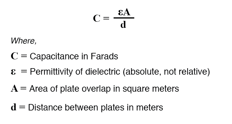
So to have a reduced Characteristic impedance we need higher capacitance. and to do that we need to bring the planes close by, ‘d’ is the distance between the plates.
So to conclude to have a good transmission line, a path to conduct the energy, the Characteristic impedance of the line should be kept to a minimum, to achieve this, we need to keep the inductance low and capacitance high. This can be achieved by keeping the signal close to a good reference plane or trace. (better call return path for the energy) . This can greatly help with Signal integrity, control all kinds of noises and reduce EMI problems.
How Energy actually travels in a PCB
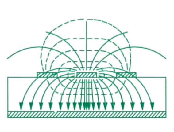
When we introduce a voltage on the conductive trace, it produces electric fields on the adjacent return plane. this pulls the electrons near the surface of the conductors. This in turns produce a Magnetic filed around the trace. One miss conception that I would like to clear is that both the forward signal current and the return current are created simultaneously,
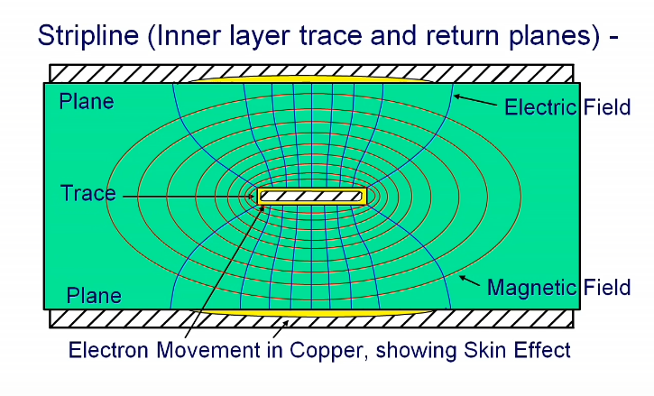
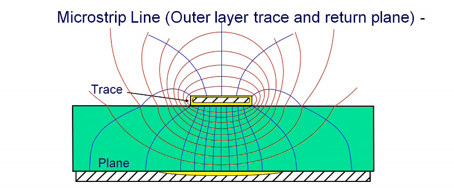
when using the outer layer some of the fields are expanded outside. But general this will not cause EMI EMC issues as these are normally under allowed limits. But be aware that coupled with a reference place break, this can be a major factor to cause an EMI issue.
so to conclude we should expect more cross talk, more interface on the outer layer than the inner layer counter part. so to keep the EMI or interfaces low keep sufficient spacing for the signals on the outer layer so that this can be avoided. Typically we want to route all highspeed signals on the inner layer to reduce losses and coupling.
Also, avoid going to the inner layers for highspeed signals if the length of the trace is less than the critical length. (Refer part1 ).
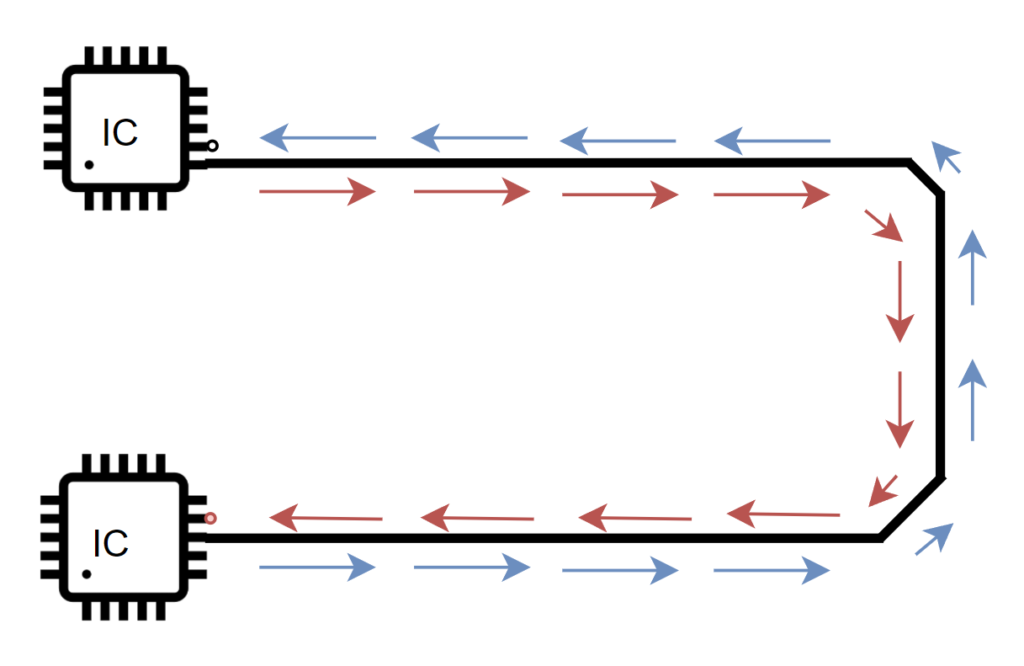
Consider the below example image, what is the expected return path of the current for this circuit. consider that its a 2 layer board with signals on the top layer and the bottom layer is fully ground.
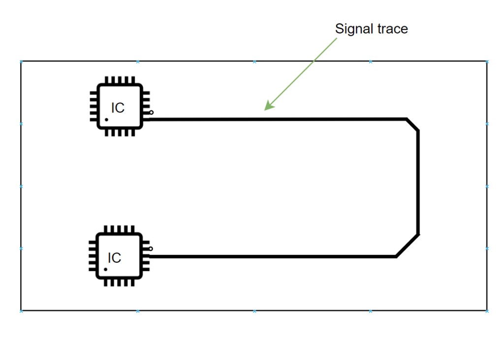
From what we learned from college, the current will always take the shortest path of impedance (resistance). This flow below might be our first guess. But sadly that’s not how the signal flow works. What we have thought is correct, only for dc or signals with extremely low frequencies.
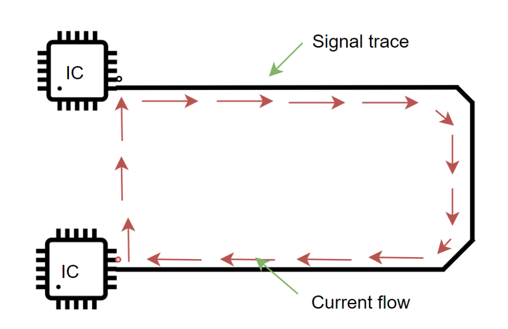
Remember the equation for characteristic impedance, when the frequency is zero, the L and C components are not there. and the path is only defined by the resistance R.

To understand the effect in detail, Check this paper by Bruce Archambeault [ link -> ] on Resistive vs. Inductive Return Current Paths. To quote the summary from the study
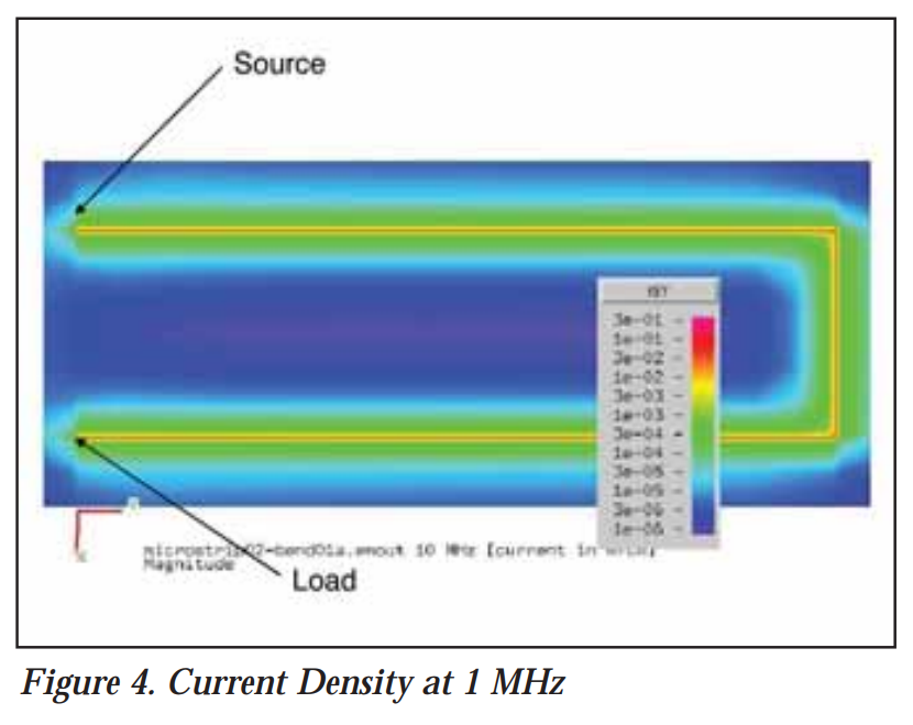
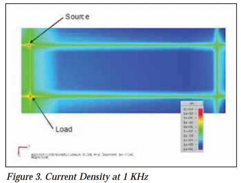
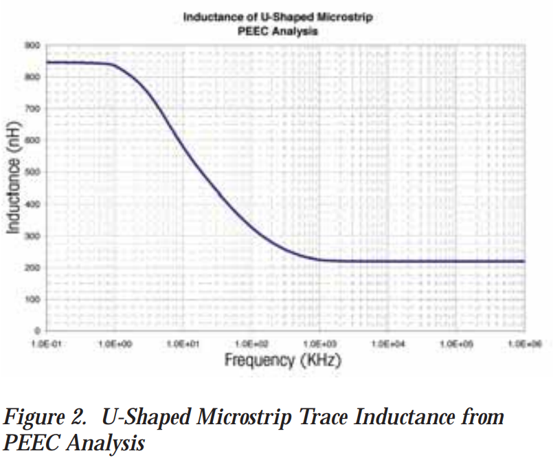
The return current path will always find the path of least impedance. This impedance will be dominated by inductance at high frequencies. The low frequency inductance can be calculated to a first order approximation with a simple rectangular loop formula and the high frequency inductance can be found using a standard per-unit-length approach. The frequency where the inductance begins to dominate over the resistance is very low, usually in the low KHz range.”
Bruce Archambeault – SUMMARY
To summarize any signal above the audio range, we can know for a fact, that it will return back through an adjacent return layer or path directly under the trace. If there is a breakage of the reference plane (or return path), Then the fields will expand to overcome this change in impedance. This can be one of the key reasons for EMI issues on the board.
CONCLUDE
Having a good reference plane for all your signal is the prime most important thing you need to do to reduce cross talk, noise floors, and reduce EMI EMC issues. So when we split our ground planes beware this can be the prime suspect for all your noise and EMI troubles.
We will look more on how PCB layer material causes EMC issues, stack up definitions, Terminations, controlled impedance paths, etc are vital for good design in future articles.
Be First to Comment